7483 Full Adder Circuit Diagram 15 Full Adder Pin Diagram
Circuit diagram for 4 bit binary adder using ic 7483 Design and implement 9's complement circuit using ic-7483 Circuit diagram for 4 bit binary adder using ic 7483 » wiring core
(Solved) - The 4 bit adder/subtractor circuit implemented with IC 7483
Circuit diagram for 4 bit binary adder using ic 7483 wiring digital 7483 ic 4-bit binary full adder with fast carry Circuit diagram for 4 bit binary adder using ic 7483
Circuit diagram of full adder 7483 logic
7483 full adder circuit diagram74hc83 full adder ic pinout, datasheet, equivalent working, 54% off Design and implementation of 10’s complement circuit using ic-74837483 full adder circuit diagram circuit diagram.
Circuit diagram for 4 bit binary adder using ic 7483Four bit adder or subtractor using 7483 Circuit diagram for 4 bit binary adder using ic 74834 bit binary subtractor circuit diagram » schema digital.

15 full adder pin diagram
7483 adder full circuit bit binary addition nap parallel requires note7483 full adder circuit diagram Circuit diagram for 4 bit binary adder using ic 74837483 full adder pdf.
Circuit diagram for 4 bit binary adder using ic 7483Four bit adder or subtractor using 7483 7483 circuit diagram full adder74hc83 full adder ic pinout, datasheet, equivalent working, 57% off.

Circuit diagram for 4 bit binary adder using ic 7483
Circuit diagram for 4 bit binary adder using ic 74837483 full adder circuit diagram Circuit diagram for 4 bit binary adder using ic 7483 » wiring core7483 circuit diagram full adder.
7483 circuit diagram full adderCircuit diagram for 4 bit binary adder using ic 7483 » wiring core Design and implementation of a bcd adder circuit using ic-7483Ic 7483 internal circuit diagram.

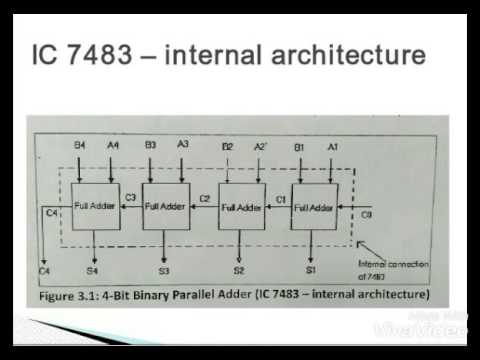
Ic 7483 Internal Circuit Diagram

Circuit Diagram For 4 Bit Binary Adder Using Ic 7483 Wiring Digital

Design And Implementation of a BCD Adder Circuit Using IC-7483

Circuit Diagram For 4 Bit Binary Adder Using Ic 7483 - Wiring Diagram

7483 Circuit Diagram Full Adder

74HC83 Full Adder IC Pinout, Datasheet, Equivalent Working, 54% OFF

7483 Full Adder Circuit Diagram - Circuit Diagram

Circuit Diagram For 4 Bit Binary Adder Using Ic 7483 - Wiring Flow Line

(Solved) - The 4 bit adder/subtractor circuit implemented with IC 7483